

The copper busbar, undertakes more than 90% of the high-load power transmission tasks. This article analyzes nine core dimensions to reveal the key role of the electroplating process in improving the performance of copper busbars. Data show that tinned copper busbar reduces resistivity by 12%-15%, improves corrosion resistance by more than 3 times, and reduces energy loss by 23% in BESS energy storage systems. This article will combine the International Electrotechnical Commission (IEC) standards and cutting-edge application cases to analyze the technical advantages and industrial value of copper-plated busbar.
I. Functions and Characteristics of Copper Busbar
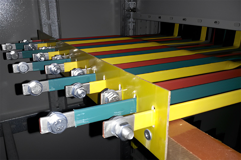
As the backbone material for power transmission, copper busbar has three core functional systems:
| Functional Dimension | Technical Indicators | Application Scenarios |
|---|---|---|
| الموصلية | Resistivity ≤ 0.017Ω-mm²/m | High Voltage Switchgear |
| Mechanical Strength | Tensile Strength ≥200 MPa | Wind Turbine Converters |
| Thermal Stability | Temperature Resistance Class ≥130℃ | Data Center Distribution |
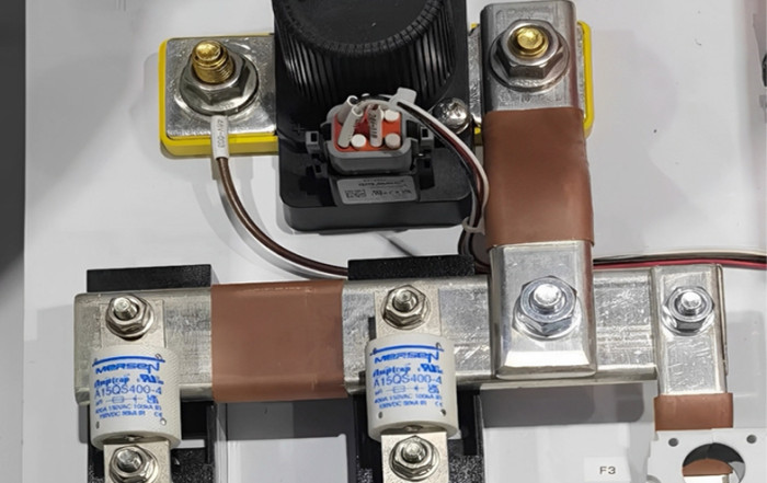
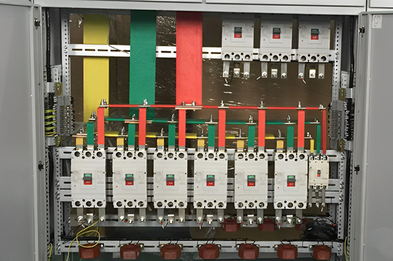
In 40.5 kV switchgear, tubular copper busbars can reduce the distance between phases by 30% due to their uniform electric field characteristics, enabling equipment miniaturization. Semiconductor industry data show that the copper plating process can reduce TSV through-hole resistance by 40%, significantly improving chip interconnect reliability.
II. Analysis of the need for plating process
1 Anti-oxidation revolution
Bare copper is exposed to air for 72 hours, which produces a 0.5-1.2 μm oxide layer, resulting in an increase in contact resistance of 18%-25%. Tin plating layer forms a dense protective film of 3-5 μm and maintains a surface resistivity of ≤0.02 Ω-mm²/m after 2000 hours of salt spray testing.
2 Cost Benefit Matrix
Comparison of the economics of different plating programs:
| Plating Material | Cost Index | Conductivity Retention | Life Cycle |
|---|---|---|---|
| Tin | 1.0 | 98% | 15 years |
| فضي | 8.2 | 99.5% | 20 years |
| النيكل | 2.3 | 99.3% | 12 years |
أنواع مواد الطلاء
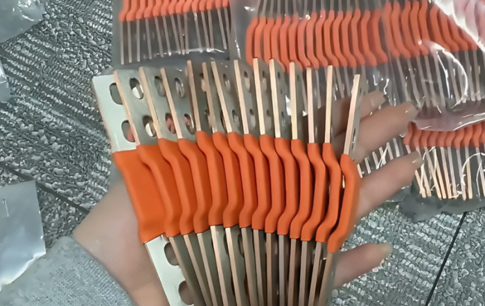
إن طلاء قضبان التوصيل النحاسية بمعادن مختلفة يمكن أن يعزز من أدائها وطول عمرها بشكل كبير. هنا، نستكشف ثلاثة أنواع شائعة من مواد الطلاء: القصدير والفضة والنيكل، إلى جانب مزاياها وتطبيقاتها.
طلاء القصدير
طلاء الفضة
طلاء النيكل
III. Plating Technology
A. Vertical Plating Process Breakthroughs
Adopting pulse reverse current technology, the deviation of plating thickness is controlled at ±0.8 μm, which is 60% higher than the traditional process. The latest level of electroplating equipment of JetBox realizes 12 μm line width precision, which meets the requirement of 25.94% conversion efficiency of the HJT battery.
B. Seedless Layer Plating
Maiwei’s innovative solution eliminates the preparation of PVD seed layer and directly deposits the copper layer through an acid plating solution, which reduces the manufacturing cost by 18% and has made a breakthrough in industrialization in the field of photovoltaic.
IV. Multi-field Application Evidence
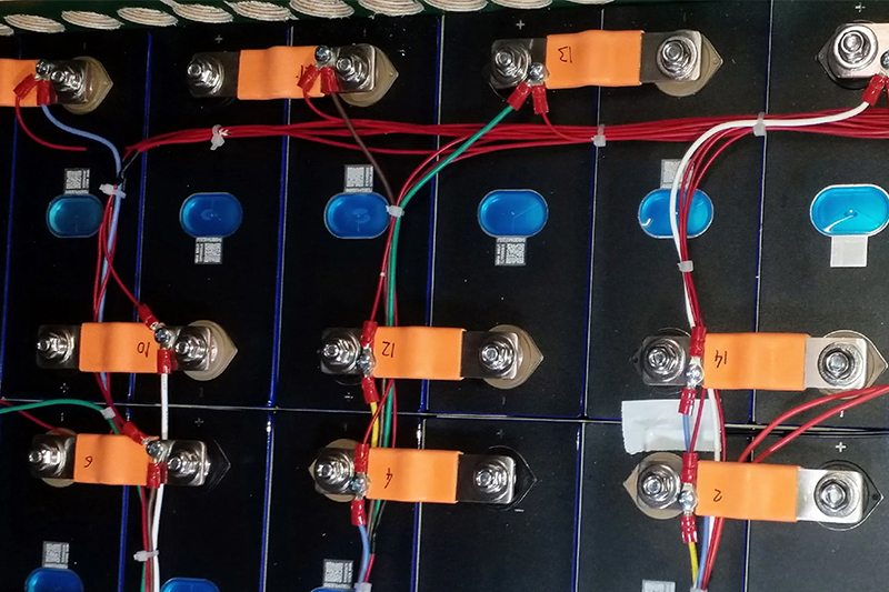
1 Energy Storage System (BESS) Revolution
The use of tinned copper busbar in Tesla Megapack 2.0 has increased the energy density of the system to 450 Wh/L, with a cycle efficiency of 92.5%. According to Wood Mackenzie, this technology drives the ROI of global energy storage projects to 8.7%.
2 Semiconductor Packaging Advancement
TSV silicon via holes are plated using a copper sulfate plating process to achieve 100% void-free filling of 5 μm diameter via holes. Applied Materials data shows that this technology has increased 3D NAND storage density to 1.2Tb/cm².
V. Environmental Benefits and Sustainability
The copper-plating process enables the busbar recycling rate to reach 98%, reducing mineral consumption by 35% compared with the traditional process. The EU Circular Economy Report points out that this technology can reduce 220,000 tons of e-waste generated annually, corresponding to a reduction of 1.5 million tons of CO₂ emissions.
خاتمة
Copper-plated busbar technology is reshaping the global energy transmission landscape. From kilowatt-scale power distribution in data centers to gigawatt-scale energy storage plants, from micron-scale chip interconnections to 100-meter-scale wind power arrays, this seemingly traditional process continues to be a modern innovation. It is recommended to pay attention to the upcoming AAC 2025 Conference to obtain cutting-edge technology dynamics.
Through the systematic demonstration of 9 dimensions, the copper plating process not only improves the material performance but also promotes the synergistic evolution of power electronics, new energy, semiconductors, and other strategic industries. In the context of carbon peaking, this technology will become the core support for smart grid construction, and the global market size is expected to maintain a CAGR of 12.7% from 2025 to 2030.
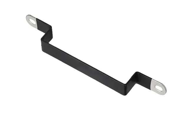
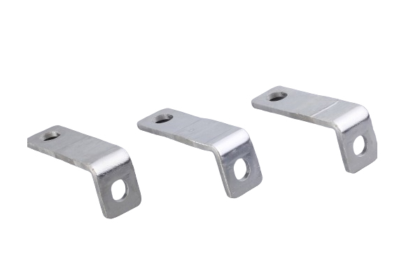
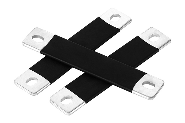
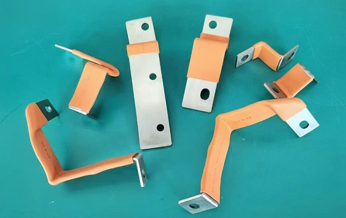
Product Categories
〉 قضيب ناقل من النحاس المطلي بالقصدير
〉 قضيب ناقل من النحاس المطلي بالنيكل
〉 قضيب ناقل من النحاس المطلي بالفضة
Related Post
Why can’t a copper busbar and an aluminum busbar be directly connected?
[email protected]2025-12-08T02:54:03+00:00ديسمبر 8th, 2025|0 Comments
Introduction Copper busbars and aluminum busbars are the two most commonly used conductive materials in the field of power systems and industrial distribution. Due to differences in cost, resource availability, and technical requirements, they often
How to Prepare for a Big Win at Tez888 Casino
Developer Ismail2025-10-04T21:44:04+00:00أكتوبر 4th, 2025|0 Comments
When aiming for a significant payout at Tez888 casino, one crucial step often overlooked is thorough receipt checking and verification. Properly managing your transaction records not only ensures transparency but also plays a vital role
Tips and Tricks for Successful Betting on Bettilt
Developer Ismail2025-08-17T05:29:18+00:00أغسطس 17th, 2025|0 Comments
When engaging in online betting, particularly on platforms like bettilt, it's crucial to incorporate strategies such as receipt checking, tax optimization, and thorough verification to maximize your success. These elements ensure that your betting activities

How Do You Calculate the Size of a Copper Busbar?
[email protected]2025-06-06T06:54:57+00:00يونيو 6th, 2025|0 Comments
1. Introduction to Busbar Sizing Accurate copper busbar sizing is vital for secure, dependable, and effective electric circulation. Busbars disperse high currents in switchgear and panelboards. Inappropriate sizing reasons extreme warmth, power loss, voltage
10 Essential Tips for Working with Copper Busbars
[email protected]2025-06-03T06:35:28+00:00يونيو 3rd, 2025|0 Comments
In modern power systems, copper busbars have actually become a core element in power transmission and distribution because of their superb electric conductivity, rust resistance and mechanical strength. As a specialist manufacturer of copper
A Guide to Maintaining Copper Busbars Effectively
[email protected]2025-05-28T06:09:36+00:00مايو 28th, 2025|0 Comments
As a core component of power transmission systems, copper busbars are an important choice for industry due to their high electrical conductivity, corrosion resistance and mechanical strength. However, the durability of its performance is
تواصل معنا
نحن نقدم أي قضبان ناقلة مخصصة
منشورات ذات صلة
Nam lacinia arcu tortor، nec luctus nibh dignissim eu nulla sit amet Maximus.

Nam lacinia arcu tortor، nec luctus nibh dignissim eu nulla sit amet Maximus.
Nam lacinia arcu tortor، nec luctus nibh dignissim eu nulla sit amet Maximus.
Nam lacinia arcu tortor، nec luctus nibh dignissim eu nulla sit amet Maximus.